- 您现在的位置:买卖IC网 > Sheet目录3871 > PIC18F1230T-I/SO (Microchip Technology)IC PIC MCU FLASH 2KX16 18SOIC
PIC18F1230/1330
2009 Microchip Technology Inc.
DS39758D-page 279
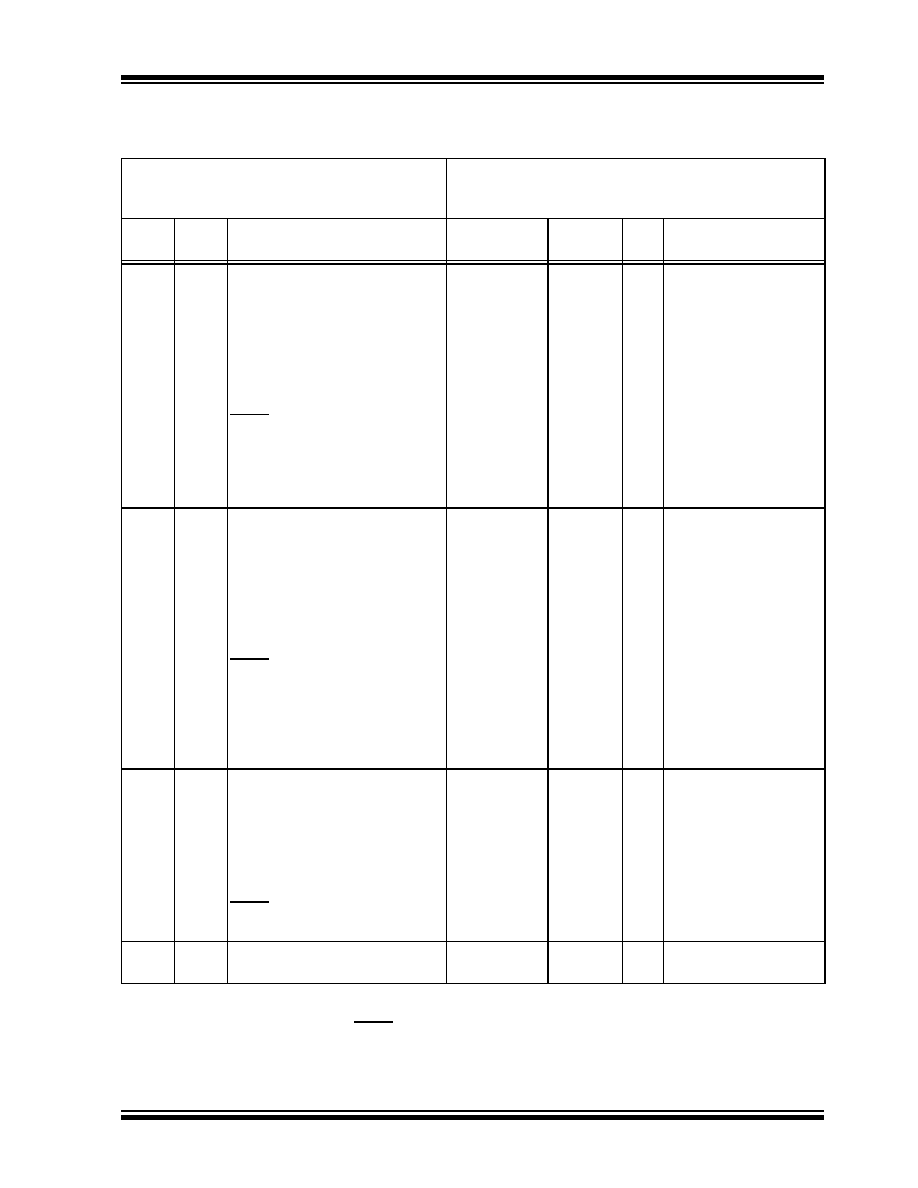
23.3
DC Characteristics: PIC18F1230/1330 (Industrial)
PIC18LF1230/1330 (Industrial)
DC CHARACTERISTICS
Standard Operating Conditions (unless otherwise stated)
Operating temperature -40°C
TA +85°C for industrial
-40°C
TA +125°C for extended
Param
No.
Symbol
Characteristic
Min
Max
Units
Conditions
VIL
Input Low Voltage
I/O ports:
D030
with TTL buffer
VSS
0.15 VDD
VVDD < 4.5V
D030A
—
0.8
V
4.5V
VDD 5.5V
D031
with Schmitt Trigger buffer
VSS
0.2 VDD
V
D031A
RC3 and RC4
VSS
0.3 VDD
VI2C enabled
D031B
VSS
0.8
V
SMBus enabled
D032
MCLR
VSS
0.2 VDD
V
D033
OSC1
VSS
0.3 VDD
VHS, HSPLL modes
D033A
D033B
D034
OSC1
T1CKI
VSS
0.2 VDD
0.3
V
RC, EC modes(1)
XT, LP modes
VIH
Input High Voltage
I/O ports:
D040
with TTL buffer
0.25 VDD + 0.8V
VDD
VVDD < 4.5V
D040A
2.0
VDD
V4.5V
VDD 5.5V
D041
with Schmitt Trigger buffer
0.8 VDD
VDD
V
D041A
RC3 and RC4
0.7 VDD
VDD
VI2C enabled
D041B
2.1
VDD
I2C enabled
D042
MCLR
0.8 VDD
VDD
V
D043
OSC1
0.7 VDD
VDD
VHS, HSPLL modes
D043A
D043B
D043C
D044
OSC1
T1CKI
0.8 VDD
0.9 VDD
1.6
VDD
V
EC mode
RC mode(1)
XT, LP modes
IIL
Input Leakage Current(2,3)
D060
I/O ports
—
200
nA
VSS < 5.5V
Vss
VPIN VDD
Pin at high-impedance
50
nA
VSS < 3V
Vss
VPIN VDD
Pin at high-impedance
D061
MCLR
—
1
AVss VPIN VDD
D063
OSC1
—
1
AVss VPIN VDD
IPU
Weak Pull-up Current
D070
IPURB
PORTB weak pull-up current
50
400
AVDD = 5V, VPIN = VSS
Note 1:
In RC oscillator configuration, the OSC1/CLKI pin is a Schmitt Trigger input. It is not recommended that the
PIC device be driven with an external clock while in RC mode.
2:
The leakage current on the MCLR pin is strongly dependent on the applied voltage level. The specified
levels represent normal operating conditions. Higher leakage current may be measured at different input
voltages.
3:
Negative current is defined as current sourced by the pin.
发布紧急采购,3分钟左右您将得到回复。
相关PDF资料
PIC18F1330T-I/ML
IC PIC MCU FLASH 4KX16 28QFN
PIC18F65J50T-I/PT
IC PIC MCU FLASH 16KX16 64TQFP
PIC18F83J11T-I/PT
IC PIC MCU FLASH 4KX16 80TQFP
PIC16LF627-04/P
IC MCU FLASH 1KX14 COMP 18DIP
PIC18F86J55T-I/PT
IC PIC MCU FLASH 48KX16 80TQFP
PIC18F43K22-I/MV
MCU PIC 8KB FLASH 40QFN
PIC16C55A-04I/P
IC MCU OTP 512X12 28DIP
PIC18LF43K22-I/MV
MCU PIC 8KB FLASH 40UQFN
相关代理商/技术参数
PIC18F1230T-I/SS
功能描述:8位微控制器 -MCU 4KB Flash 256 RAM RoHS:否 制造商:Silicon Labs 核心:8051 处理器系列:C8051F39x 数据总线宽度:8 bit 最大时钟频率:50 MHz 程序存储器大小:16 KB 数据 RAM 大小:1 KB 片上 ADC:Yes 工作电源电压:1.8 V to 3.6 V 工作温度范围:- 40 C to + 105 C 封装 / 箱体:QFN-20 安装风格:SMD/SMT
PIC18F1320-E/ML
功能描述:8位微控制器 -MCU 8KB 256 RAM 16 I/O RoHS:否 制造商:Silicon Labs 核心:8051 处理器系列:C8051F39x 数据总线宽度:8 bit 最大时钟频率:50 MHz 程序存储器大小:16 KB 数据 RAM 大小:1 KB 片上 ADC:Yes 工作电源电压:1.8 V to 3.6 V 工作温度范围:- 40 C to + 105 C 封装 / 箱体:QFN-20 安装风格:SMD/SMT
PIC18F1320-E/P
功能描述:8位微控制器 -MCU 8KB 256 RAM 16 I/O RoHS:否 制造商:Silicon Labs 核心:8051 处理器系列:C8051F39x 数据总线宽度:8 bit 最大时钟频率:50 MHz 程序存储器大小:16 KB 数据 RAM 大小:1 KB 片上 ADC:Yes 工作电源电压:1.8 V to 3.6 V 工作温度范围:- 40 C to + 105 C 封装 / 箱体:QFN-20 安装风格:SMD/SMT
PIC18F1320-E/SO
功能描述:8位微控制器 -MCU 8KB 256 RAM 16 I/O RoHS:否 制造商:Silicon Labs 核心:8051 处理器系列:C8051F39x 数据总线宽度:8 bit 最大时钟频率:50 MHz 程序存储器大小:16 KB 数据 RAM 大小:1 KB 片上 ADC:Yes 工作电源电压:1.8 V to 3.6 V 工作温度范围:- 40 C to + 105 C 封装 / 箱体:QFN-20 安装风格:SMD/SMT
PIC18F1320-E/SS
功能描述:8位微控制器 -MCU 8KB 256 RAM 16 I/O RoHS:否 制造商:Silicon Labs 核心:8051 处理器系列:C8051F39x 数据总线宽度:8 bit 最大时钟频率:50 MHz 程序存储器大小:16 KB 数据 RAM 大小:1 KB 片上 ADC:Yes 工作电源电压:1.8 V to 3.6 V 工作温度范围:- 40 C to + 105 C 封装 / 箱体:QFN-20 安装风格:SMD/SMT
PIC18F1320-H/ML
功能描述:8位微控制器 -MCU 8KB FL 256RAM 16 I/O RoHS:否 制造商:Silicon Labs 核心:8051 处理器系列:C8051F39x 数据总线宽度:8 bit 最大时钟频率:50 MHz 程序存储器大小:16 KB 数据 RAM 大小:1 KB 片上 ADC:Yes 工作电源电压:1.8 V to 3.6 V 工作温度范围:- 40 C to + 105 C 封装 / 箱体:QFN-20 安装风格:SMD/SMT
PIC18F1320-H/P
功能描述:8位微控制器 -MCU 8KB FL 256RAM 16 I/O RoHS:否 制造商:Silicon Labs 核心:8051 处理器系列:C8051F39x 数据总线宽度:8 bit 最大时钟频率:50 MHz 程序存储器大小:16 KB 数据 RAM 大小:1 KB 片上 ADC:Yes 工作电源电压:1.8 V to 3.6 V 工作温度范围:- 40 C to + 105 C 封装 / 箱体:QFN-20 安装风格:SMD/SMT
PIC18F1320-H/SO
功能描述:8位微控制器 -MCU 8KB FL 256RAM 16 I/O RoHS:否 制造商:Silicon Labs 核心:8051 处理器系列:C8051F39x 数据总线宽度:8 bit 最大时钟频率:50 MHz 程序存储器大小:16 KB 数据 RAM 大小:1 KB 片上 ADC:Yes 工作电源电压:1.8 V to 3.6 V 工作温度范围:- 40 C to + 105 C 封装 / 箱体:QFN-20 安装风格:SMD/SMT